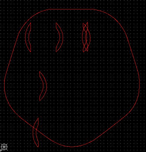
So I modified the new Raspberry Pi connector @vanepp made so that I can ensure the board, mounting holes, and GPIO header pins all perfectly align (there are very slim margins!).
What I did was took his great part, and then added a board, and mount holes, in the sub mm perfect places, great work around I thought! I delete the ‘board’ group when I add the SVG to the pi connector part, and I delete the silkscreen and copper layers when I add the PCB Board design to Fritzing, I then set both the board and the part in the PCB view of Fritzing to exactly 0.000 (though there’s also a minor issue there too - for some reason they never actually take 0.00 on the x axis, they are either -0.001 or 0.003, but never more than 0.003 off what I want.
![pi board pcb_master_ink]()
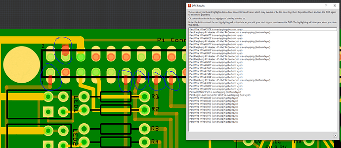
My Main issue, however, is that when I do my DRC when I think it’s all done it complains that traces are going over the pads that @vanepp made, but they didn’t when I used his part without modifications so I’m quite confused by that. I did nest copper layers, so just one, inside copper1 and 0, but I’ve also tried it with the two layers that @vanepp originally made, and that too brings the same issue on DRC.
Here’s the problem according to DRC:
Here’s the project that the above screenshot is from: Door Pi.fzz (197.4 KB)
Here’s the post where @vanepp submitted his part to the forum: Raspberry Pi 40pin Header and this is the part I’m using: https://forum.fritzing.org/uploads/short-url/vjZD8e7vWQOK6oFjDyglJsGaKZc.fzpz
Sorry guys, I really thought I had got a real handle on Fritzing now but this has quite thrown me.
If you’re able to help, that would be epic!
Thanks, James.
1 post - 1 participant
Read full topic


