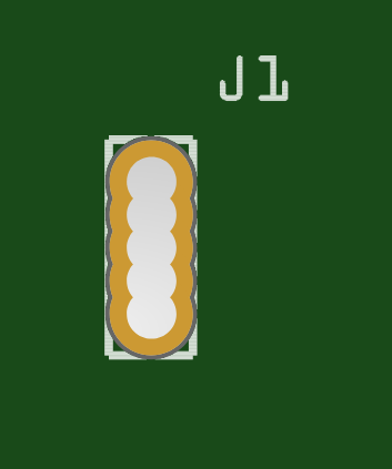
This is what I mean with plated-through slots.
I recently managed to desing a pcb with plated-through slots to solder a Li-ion 18650 battery with soldered nikel U-tags.

To achieve such thing I had to design 2 things:
1st → A custom pcb svg with pads
2nd → li-ion part footprint with platted slots
Then I had to make both things match in the pcb layout. If I wanted to move the li-ion battery position in the layout, I had to redesign the custom pcb svg. It was a pain in the a@#.
Before reaching this point, I ried to modify li-ion footprint svg with “<path…” instead of “<circle…” in cooper layers, but fritzing wont generate the correct gerber file. I guess fritzing only understands drills when you use circles in cooper layers.
I also tried several drills together, but it is a horrible work-arround and most PCB manufacturers wont accept that solution as it can break the drill.
Don’t do this please:
So the question is:
¿Is there a way to desing a part that produces those plated-through slots in the gerber?
2 posts - 2 participants